Sustainability
We have been taking over the manufacturing of specific circuits for our customers for 15 years. Our holistic model of ensuring the cost-efficient production of long-lasting semiconductors according to different quantity requirements has proved itself in practice. High rates of on-time delivery and exceptional quality when supplying components are our strengths.
Industrial sustainability is our trademark. By a strict selection of used subcontractors and technologies, we guarantee the availability of all our ASICs during 10 years. For medical, air or rail transport applications, power plant control, for which life-time in operational conditions goes far beyond 20 years, we propose extension solutions. We also offer technological migration, portages and silicon storage in order to support your systems with enough units through their end-of-life period.
Last but not least, we keep an eye on strategic procurements with the duplication of each operation of the supply chain when possible; thus we are able to activate back-up solutions on demand in case of any force-majeure event.

Full and partial flow
Full production offering
ID MOS manages the whole production flow. The operations are followed up in real time, including the logistical flow and the Quality insurance.
Our mission is to produce. If you already carried out the development of your own IC(s), we may propose to perform its qualification and industrialization, and later on ensure the supply chain management including prototyping and pre-series. The circuit may be delivered with the same service and quality as if it had been designed in one of our Design Centers. Specific suppliers, pre-qualified or pre-selected on your side may be integrated in the production flow.
ID MOS SCM services involve a large choice of mixed-signal technologies ranging from 1µm down to 65nm, able to answer to most of the power-supply domains, high voltage, non-volatile and random-access memories and very low power consumption requirements.
The packaging is performed by our state-of-the-art partners, gathering the ability of Chip-On-Board (COB) and conventional plastic packaging such as DIP, SOP, QFB, SOT, LCC, BGA, QFN and all CSP variations. For harsh environments, ceramic packaging is proposed.
Partial flow
Using the flexibility of our SCM, we may also offer to manage for your account only particular manufacturing steps like wafer sourcing+probing or packaging+final test.
The test operations (probing and/or final test) may be realized under your specification. ID MOS will integrate your product in their logistical and Quality procedure.
Quality Assurance
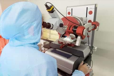
The microchip final test is the very last electrical verification of your ASIC. It guarantees the chip integrity though plastic encapsulation and allows temperature testing. This last control, complementary to the wafer test, takes part of the global testability strategy ensuring a global coverage in the end. In the same way as wafer probing, Final Test is prescribed by the project team during the chip design and deployed by the test-engineering department, on various platforms.
Monitoring the quality of manufacturing is consolidated by IDMOS’ own Product and Quality Insurance teams. The control of production indicators is done in real-time, with each involved subcontractor, on a by-lot basis. The whole manufacturing process is organized upon control-card monitoring, for which automatic alert levels are revised quarterly.
Continuous improvement principles are handled by local Product Managers, who monitor indicator trends, investigate issues related to marginal lots and generate pre-delivery certificates, under the direct supervision of ID MOS Product team.
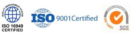
All our Production subcontractors are ISO9001, ISO14001 certified, and ISO/TS16949 for the most strategic ones. ID MOS regularly conducts quality and line audits in order to better master the processes and minimize the product risks.
Continuous improvement is managed by action plans at each production steps in order with the strong philosophy of improving productivity and quality level.
In many application fields, especially automotive, avionics or medical, the circuit Qualification is required prior to any production launch. Based on AECQ10, JEDEC or ESCC9000 standards, we apply the related specific test flows on the microchips.
Our test facilities include pre-conditioning, tests in high-stress environment ((TC, HAST, ESD, EOS) and accelerated aging tests (burn-in, ELFR, HTOL). Deviations and failures are recorded and analyzed with the active support of SERMA Technologies laboratory, in the process of minimizing the manufacturing defect rate.
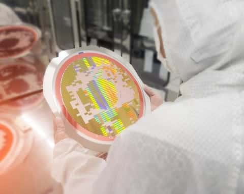
During the manufacturing of the microchip, the foundry controls its process parameters by performing several pre-delivery parametric measurements on each wafer. Downstream of the production process, we make a comprehensive functional and parametric test in order to guarantee the product performances. Performed at wafer level (EWS), this die-unitary test allows parametric recording and further analysis techniques such as statistical sorting (part average testing), as part of the global zero-defect process.
The wafer probing is the outcome of our ASIC design methodology « design for testability », which integrates in each microcircuit a dedicated set of devices for in situ test (BIST) or specific architectures to enhance external tester verifications. During that manufacturing operation, calibration or individual customization can take place.